Tolk's group

Research
Depth and defect density dependence of optical constants in H implanted 4H-SiC
|
We have measured depth dependent profile of the complex refractive index of proton irradiated SiC at low fluences using coherent acoustic phonon (CAP) spectroscopy. The increase in the real part of the refractive index is shown to have nonlinear dependence on defect concentration whereas the increase in the imaginary part linearly increases with defect concentration. These studies provide basic insight into the dependence of optical properties of 4H silicon carbide on defect densities created by ion bombardment, which is of relevance to the fabrication of SiC-based photonic, optoelectronic devices and degradation of SiC based devices in space. http://dx.doi.org/10.1063/1.4945443
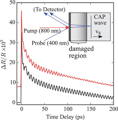
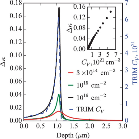
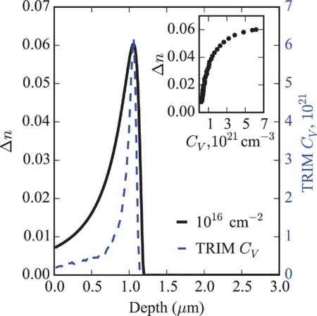
Figure. (Left) Typical CAP response for implanted (red) and unimplanted (black) n-type 4H-SiC. Inset: CAP experiment configuration showing strain-wave induced self-interference in the probe reflectivity. (Middle) Observed changes in the extinction coefficient as a function of depth using CAP, following hydrogen implantation. The inset shows the implantation induced extinction coefficient change versus vacancy concentration. (Right) Observed changes in the real part of the refractive index as a function of depth using CAP, following hydrogen implantation. |
CAP interferometry to determine the optical modification in ion-implanted diamond crystals
 Diamond is well known for its superlative mechanical, electronic, thermal, and tribological properties. Most recently, diamond’s optical properties have generated considerable interest in photonics applications due to diamond’s many optically active defect complexes. Recently, an ion implantation and lift-off technique in diamond has been reported for the fabrication of nanoscale photonic devices, and ion implantation has also been used to form NV– centers. Ion implantation in crystals introduces defects into the lattice that modify local electronic wave functions and thereby modulate the opto-electronic properties of the material. In addition, ion implantation in diamond can transform the bonding characteristics of the lattice atoms, introducing significant strain in implanted crystals and, in some instances, causing surface swelling. Reliable fabrication of single-photon emitting centers and photonic devices in diamond will require a detailed understanding of the associated defects created within the lattice during the implantation process.
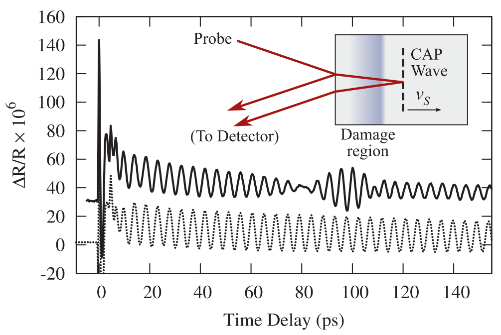
We have used coherent acoustic phonon interferometry as a sensitive tool for studying the implantation damage-induced modification to the opto-electronic nature of diamond lattices. Our results show a fluence-dependent decrease in the real part of the refractive index under ion implantation, an increase in the imaginary part, and a sign reversal in the photoelastic coefficient.
http://dx.doi.org/10.1063/1.4765647 |
Multiphoton Absorption in Semiconductor Crystals
|
Multiphoton absorption in semiconductors is a process involving the nearly-simultaneous absorption of two or more photons by a semiconducting material when the energy of a single photon is insufficient to excite an electron-hole pair. Generally, high-intensity optical pulses are required.
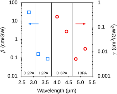
In recent work, we have measured the multiphoton absorption characteristics of germanium using the Vanderbilt Free Electron Laser (FEL) at a variety of mid-IR wavelengths. Computer simulations of the pulse propagation and resultant carrier concentrations enable the determination of the absorption coefficients at each wavelength. This work was supported by the National Science Foundation under grant NSF CHE‐0707044, and will soon be published in Physical Review B.
In future work, we intend to apply Coherent Acoustic Phonon Spectroscopy to the multiphoton absorption process, enabling the depth-dependent characterization of nonlinear materials. |

Characterization of Interfacial Charge Traps using Second Harmonic Generation
|
We are characterizing interfacial charge traps in systems such as nanocrystals on TiO2, nanocrystals on Si, and boron-doped Si/SiO2 using (time-resolved pump-probe, time-dependent) linear and nonlinear optical techniques. 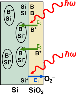 Figure, above: Photo-excited electrons can fill both empty boron-induced charge traps and surface oxygen charge traps in the boron-doped Si/SiO2 system. Graph, below: Power dependence of charge trap filling probed by time-dependent second harmonic generation. Blue trace: both traps are filled simultaneously between 10 and 178 s, and then only the oxygen traps after 266 s. Red trace: only the boron-induced charge traps are filled between 10 and 178 s, and then only the oxygen charge traps after 266 s. 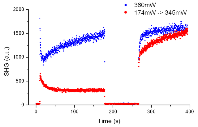 |
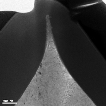
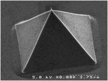
Diamond Cathode Pyramids
|
Diamond cathodes have demonstrated significant potential as electron emitters. Nanocrystalline diamond (grain size ~ 1-100 nm) possesses unique properties including deliberate and controlled amounts of sp2-carbon content and n-type electrical conductivity at room temperature occurring with nitrogen incorporation. Ultra-sharp diamond tips with a radius of curvature as small as 5 nanometers have been achieved and show significant improvement in emission characteristics compared to conventional silicon emitters. We have demonstrated electron emission from widely spaced nanodiamond pyramidal tip arrays. Partial array participation is observed at fields as low as 2.5 V/µm with most of the array participating in emission as the field increases to 5V/µm. Array tips have not been observed to be physically damaged by extended emission tests. Transmission electron microscopy (TEM) provides insight into tip structure and composition, as well as offering insight as to why morphologically identical tips do not emit equally.
 |
Characterization of Point Defects in Semiconductor Crystals using Coherent Acoustic Phonon Spectroscopy
|
Point defects are atomic-scale imperfections in otherwise periodic crystal lattices. Although small, point defects can have large effects on electronic and optical devices due to charge trapping and structural distortion. Due to their small size of less than 1 nm, characterizing and quantifying point defects, their spatial distribution, and their effect on the local optoelectronic structure is a time-consuming task. We have developed a method to quickly detect and characterize point defects using coherent acoustic phonon spectroscopy. In our experiments ultrafast laser pump pulses are absorbed at the surface of a sample and give rise to picosecond acoustic pulses which are roughly 10nm in size and travel into the bulk material at the speed of sound. We then monitor the travel of the acoustic wave using a time-delayed probe pulse. By studying exactly how the probe light interacts with the acoustic wave we can non-invasively and non-destructivley study the optical and electronic properties of our samples with 10-nm resolution. 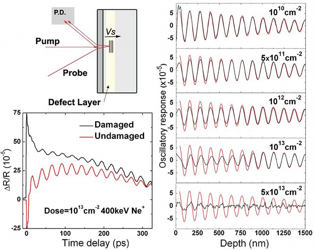 Using this technique we have shown that point defects can be detected with high precision. Further, we have developed this technique to be able to measure the spatial distribution and predict with high confidence the exact number of defects present at any point below the surface. Our experiments can detect defect concentrations to almost 1/100,000 atoms. No other technique can boast the same combination of sensitivity, depth resolution, depth limits, ease of use, and sample preservation. Currently we are studying how to extend this technique to the study of internal strain and interface properties, a common problem in thin film growth, with application in a variety of fields from photovoltaics to magnetic or spin-based information processing. Additionally, we are studying the exact interaction between defects and optical response in our experiments. By understanding the dependence between the change in optical response and number of defects, we can estimate the extent of nearest neighbor interactions that propagate outward through the electronic structure surrounding a single point defect. This can have great impact on the use of nanoscale devices, since as the size scale decreases single defects have ever increasing influence. |
Connect with Vanderbilt
©2026 Vanderbilt University ·
Site Development: University Web Communications