Silicon Photonics
Deep Subwavelength Confinement with Bowtie Photonic Crystals for Enhanced Light-Matter Interaction
Photonic crystals are made by creating periodic variations in refractive index. This periodic refractive index profile allows photonic crystals to control light much in the way crystalline atomic lattices can control the flow of electrons, which results in materials being insulating, conducting or semiconducting. Using photonic crystals to create ‘semiconductors of light’ and then designing optical trap states through introducing defects in the lattice enables strong temporal confinement of light which can be designed to meet and even surpass performance shown in optical devices like standard waveguides, ring resonators, Fabry-Perot cavities and plasmonic resonators. The illustration in Fig A1 (a) shows the spatial confinement of light in photonic crystals can be significantly increased by implementing a bowtie unit cell to create the photonic crystal. This bowtie design is a result of an iterative design process shown in Fig. A1 (b) which leverages boundary conditions from Maxwell’s equations to localize optical energy at the center of the bowtie. The bowtie photonic crystal’s demonstrated combination of spatial confinement on the order of plasmonics and temporal confinement on the order of high-quality photonics allows for ultra-high enhancement of local optical field intensities, making this an incredibly promising platform for a wide array of optical applications, including non-linear optics, phase change materials, opto-mechanics, quantum optics and optical nanomanipulation. We are currently working towards leveraging bowtie defects in 1D (Fig. A1 (c)) and 2D (Fig. A1 (d)) photonic crystal cavities to experimentally enhance performance in the aforementioned applications.
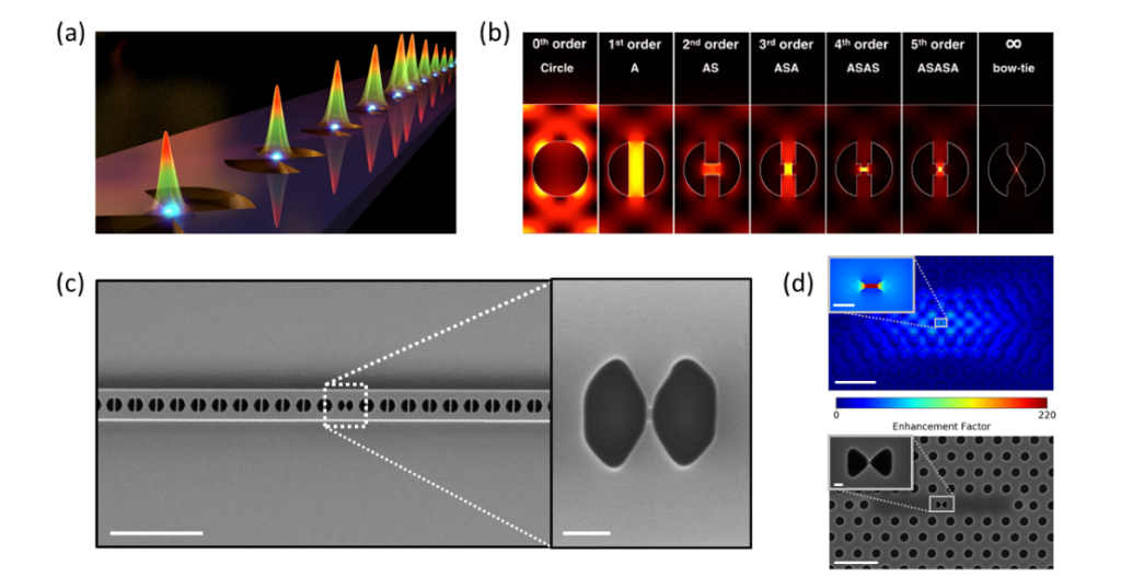
(a) Illustration of 1D bowtie photonic crystal. The bowtie tips act to confine light and greatly increase the localized optical power. (b) The bowtie design is part of an iterative process of using two orthogonal boundary conditions from Maxwell’s equations. By stacking these ‘slot’ and ‘anti-slot’ effects many times, we arrive at the bowtie shape for extreme spatial confinement of light. (c) SEM image of 1D photonic crystal cavity with a bowtie defect. Scale bars are 2um (left) and 100nm (right). (d) Simulated power enhancement for a bowtie defect in a 2D photonic crystal (top) and SEM image of a fabricated bowtie defect (bottom). Scale bars are 1um (zoomed out) and 50nm (insets).
Silicon Modulators Using Metal-Insulator Switching of Vanadium Dioxide
Silicon (Si) photonics has the potential to reduce energy consumption and increase bandwidth density in short-distance communications and information processing, with Si waveguides providing a low-loss, on-chip platform for optical signal processing. To achieve signal modulation and switching, we have been investigating a phase-change material known as vanadium-dioxide (VO2), a functional oxide undergoing metal-insulator transition (MIT) near 67C, with dramatic changes in electrical resistivity and near-infrared transmission. We present Si-VO2 hybrid optical modulators motivated by the need for compact Si-compatible optical switches operating at THz speeds. The MIT can be induced thermally, optically (by ultra-fast laser excitation in less than 100 fs), and possibly by electric field. The ultrafast switching properties of VO2 in the near-infrared can be used to tune the effective index of ring resonators at the telecommunication frequencies instead of relying on the weak electro-optic properties of silicon. In a linear geometry, we have demonstrated the potential for electrically triggering the MIT in an electro-optic absorption based modulator. For an all optical modulation scheme, we have done work with photothermal modulation in a ring resonator geometry and modulation in both linear and ring resonator geometries in response to nanosecond optical pulses. Our work with VO2-embedded silicon waveguides has demonstrated sub-picosecond switching, the fastest achieved in a silicon platform. Currently, we are pursuing methods to continue increasing device performance speed while simultaneously achieving high modulation depths and maintaining small device footprints.
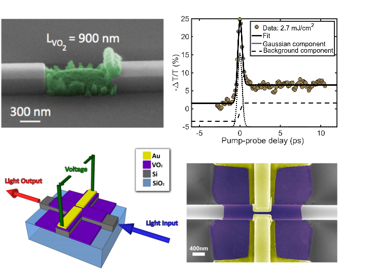
(top) Tilted SEM image of a VO2-embedded Si waveguide optical switch (VO2 is false-colored green) and sub-picosecond time response of the embedded VO2-Si optical switch, characterized by pump-probe measurements. (bottom) Schematic and SEM image of the linear absorption electro-optic modulator.